Design and Construction of a 3D Printed Smartphone-Based Spectrometer with Photonic Crystal Integration
Introduction
A spectrometer is a scientific instrument that helps us understand the composition of light. At its core, it breaks light into its component wavelengths—just like a prism creating a rainbow—and lets us analyze the intensity of each color. Why is that important? Because different materials absorb, reflect, or emit light in very specific ways. By studying these light patterns, we can identify what a substance is made of or how it behaves under certain conditions. Spectrometers are used in a wide range of fields—physics, chemistry, biology, astronomy, environmental science, and even food quality testing. For example, astronomers use them to figure out what stars are made of, and biologists use them to measure the concentration of molecules in a sample. But here’s the catch: professional spectrometers are expensive. Their high precision and durability come with a price tag that can be far out of reach for small labs, students, DIY hobbyists, or researchers in developing regions. That’s where the idea of building your own low-cost spectrometer becomes incredibly valuable.
Why Build a Low-Cost Spectrometer?
Imagine having a powerful tool for scientific analysis that costs less than a meal at a restaurant. That is exactly the promise of a do-it-yourself (DIY) spectrometer using a DVD as a diffraction grating and a smartphone as the detector. This approach is effective for several reasons:
- DVDs are already diffraction gratings: A standard DVD contains thousands of closely spaced grooves that can diffract light into its spectral components. This optical behavior mimics the function of the costly diffraction gratings used in professional-grade spectrometers.
- Smartphones have excellent cameras: Modern smartphones are equipped with high-resolution image sensors capable of detecting the intensity of different wavelengths of light. This makes them surprisingly useful for recording and analyzing spectral data.
- Accessible and affordable: The required materials—such as a DVD, a cardboard box, black tape, a razor blade for creating a slit, and a smartphone—are widely available and inexpensive. This makes the design highly accessible for students, educators, researchers in low-resource settings, and DIY science enthusiasts.
- Educational value:Constructing a spectrometer from basic components provides a hands-on opportunity to learn about optics, light behavior, data acquisition, and basic engineering principles. The learning process itself adds value beyond the functionality of the device.
- Customization and experimentation:Unlike commercial instruments, a DIY spectrometer can be easily modified. Users can tailor the setup to specific applications, such as analyzing different light sources, measuring absorbance in liquids, monitoring plant pigments, or detecting contaminants in water samples.
Apparatus and Construction
Light Source and Optical Path
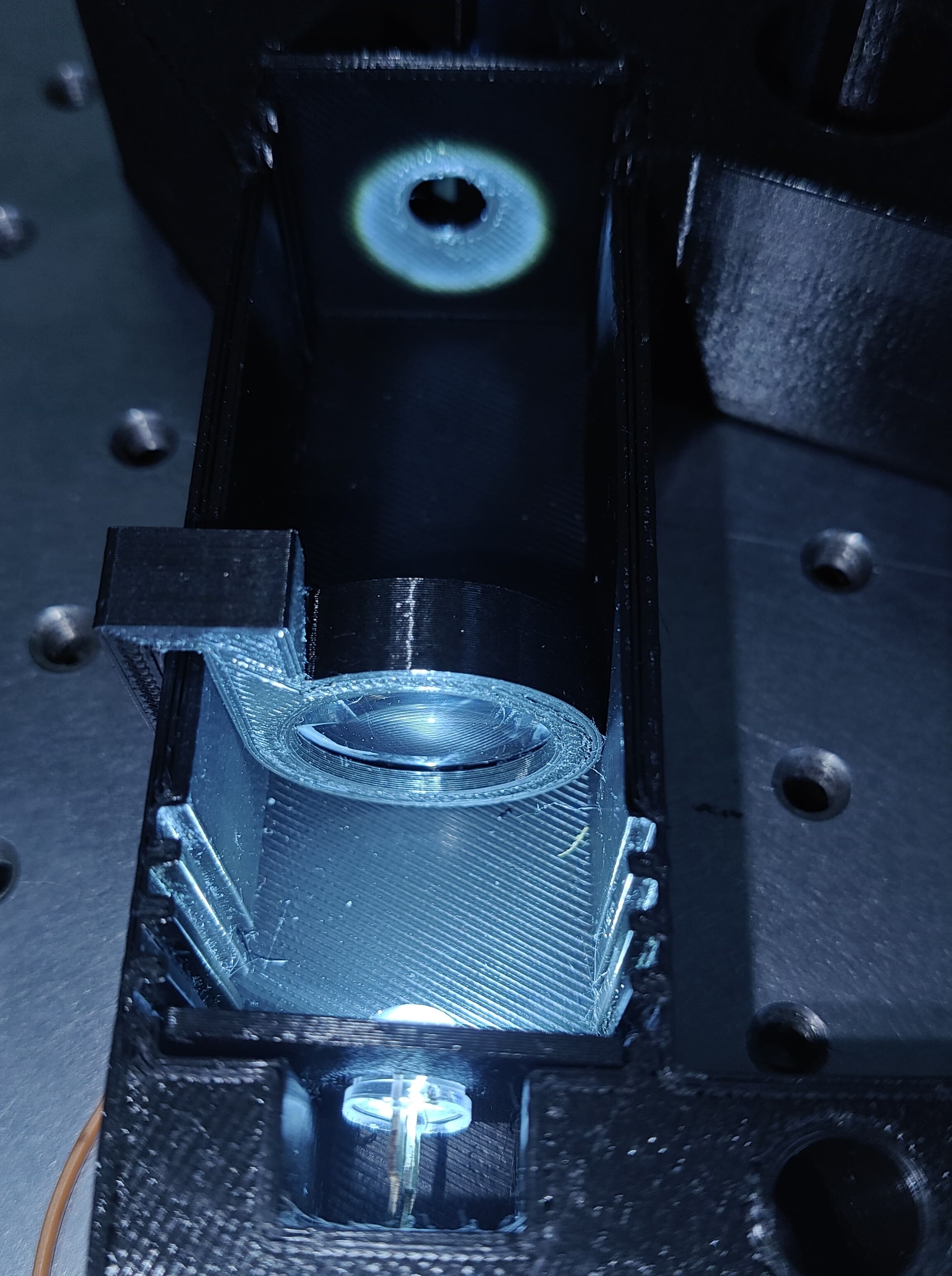
A white LED was employed as the primary light source for the spectrometer. The emitted light was initially collimated using a plano-convex lens with a focal length of 30~mm. The collimated beam passed through an aperture and was then reflected by a plane mirror towards a precision-machined slit of width 0.2~mm. The light emerging from the slit was further collimated using a second lens with a focal length of 20~mm and directed towards the diffraction grating. It is noteworthy that, for low-cost and customizable applications, these lenses can also be fabricated using polydimethylsiloxane (PDMS), a transparent elastomeric material that allows for easy molding of optical elements with good transmission in the visible range.
Diffraction Grating and Detection
The diffraction grating was obtained from the reflective layer of a standard DVD, which contains approximately 1350 lines per millimeter. The grating was positioned and tilted precisely to achieve optimal diffraction of the incoming collimated beam. The resulting spectrum was captured using a smartphone camera mounted on a fixed 3D-printed holder, ensuring stability and alignment. To enhance sensitivity and improve light collection at the camera sensor, an additional converging lens of suitable focal length and aperture can be placed directly in front of the smartphone camera. This optional component increases the intensity of the captured spectral features without compromising resolution. s
Modular Sample Holder and Adaptability
The spectrometer features a modular sample interface that supports interchangeable adapters, providing flexibility for different modes of measurement. Two primary adapters were designed: one housing a plane mirror and the other holding a cuvette for sample analysis. The mirror adapter is used for calibration and reference measurements by reflecting collimated white light directly into the grating. The cuvette holder, on the other hand, is intended for sample-based analysis, including liquid absorbance studies and advanced photonic measurements. Both adapters can be swapped without disturbing the optical alignment of the system, offering high repeatability and ease of use.
Photonic Crystal Integration
For enhanced sensitivity and advanced optical interaction studies, a photonic crystal was incorporated into the spectrometer design. The photonic crystals were fabricated using a dip-coating technique to form ordered nanostructures on a transparent substrate. This coated surface was then integrated into the cuvette, serving as one of its walls. A small prism was mounted on top of the photonic crystal to facilitate the excitation of Bloch surface waves, which are confined electromagnetic modes that propagate along the surface of the crystal. This configuration enables highly sensitive detection based on refractive index changes at the surface, making it particularly suitable for biosensing and molecular diagnostics.
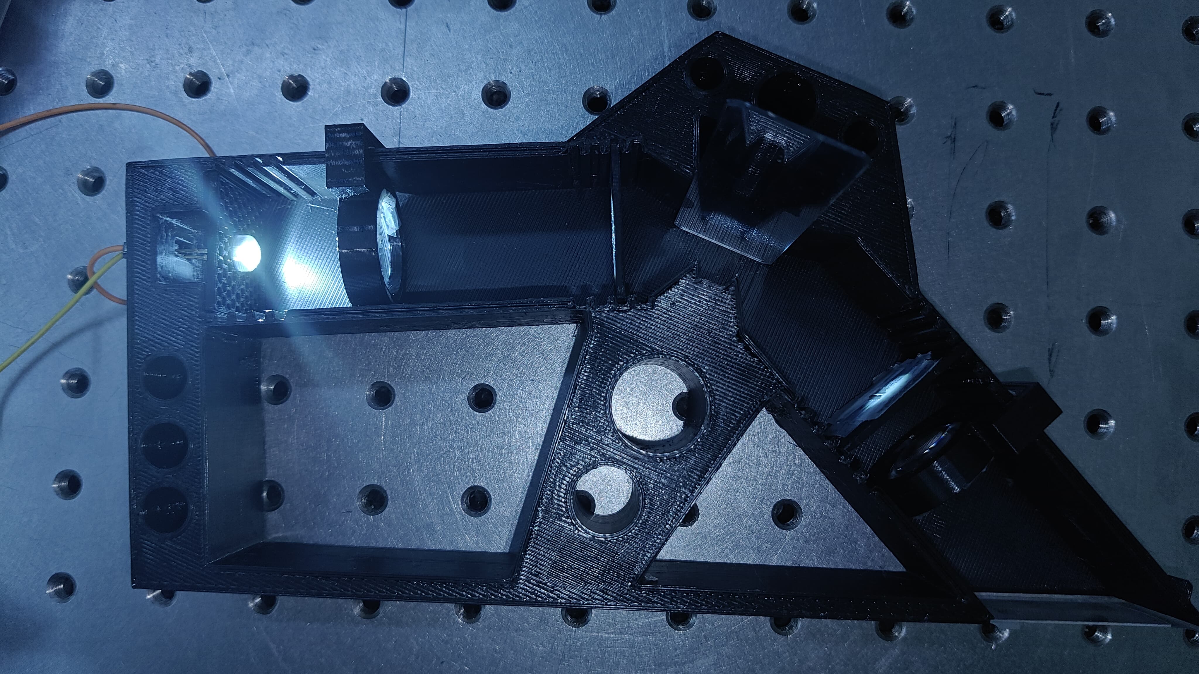
Figure 1: 3D printed spectrometer top view.
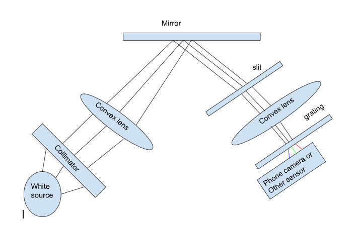
Figure 2: Schematic of the Spectrometer.
Key Concepts
Photonic Crystals
Photonic crystals are optical materials with periodic dielectric structures that affect the motion of photons. They create photonic bandgaps—frequency ranges where light propagation is prohibited. These crystals are used to manipulate light in innovative ways, including waveguiding and filtering.
Bloch Surface Waves (BSW)
BSWs are surface-confined electromagnetic waves that propagate along the interface of a photonic crystal and an external medium. Unlike surface plasmon resonance, BSWs work in dielectric structures and can provide high sensitivity and low losses, which are advantageous in sensing applications.
Soft Lithography and PDMS Use
The diffraction grating from the DVD can be transferred onto a glass substrate using soft lithography involving PDMS (Polydimethylsiloxane). PDMS can also be used to fabricate optical lenses by molding against curved surfaces. This enhances customization in DIY optical components.
Online Spectral Analysis Tool
We developed a web-based tool for spectrum analysis that allows:
- Uploading or capturing spectra using a smartphone.
- Cropping and isolating the region of interest.
- RGB-based wavelength calibration.
- Intensity vs wavelength plotting.
- Exporting plots and data as downloadable CSV files.
This tool can be accessed at: Sai Spectrum Web App
Operating Procedure of the Spectrometer
- Power On the Light Source: Begin by turning on the white light source that will be used for spectral analysis.
- Mount the Smartphone: Securely mount the smartphone in its designated position such that its camera aligns with the internal optical pathway of the spectrometer.
- Access the Web Application:Open the web-based application developed for spectrum acquisition and analysis using the smartphone browser.
- View the Direct Reflection Spectrum: Use the plane mirror adapter to reflect the incoming white light, enabling the direct capture of the spectrum by the smartphone camera.
- Calibrate the Spectrum: Identify the spectral peaks corresponding to the blue and red regions. Assign a wavelength of 450~nm to the peak in the blue region and 625~nm to the peak in the red region. This establishes a reference for accurate wavelength calibration.
- Replace with Cuvette Adapter: After calibration is complete, remove the plane mirror adapter and insert the cuvette adapter to enable absorbance measurements through the sample.
- Acquire Calibrated Spectrum: Observe the spectrum again. The web application will now display a calibrated graph based on the earlier wavelength calibration.
- Download Data: The spectrum data points can be downloaded in CSV format. In addition, the plotted spectrum can be saved as an image file. The application also allows for interactive exploration of the plotted data.
Results and Discussion
The spectrometer was able to resolve spectral components of the white LED effectively. After calibration, the intensity vs wavelength plots showed distinguishable peaks consistent with expected LED emission profiles. When a sample was placed in the path using the cuvette, absorption dips corresponding to material properties were observed. The modular design allowed seamless swapping between mirror and cuvette adapters, demonstrating potential for rapid testing. Integration with photonic crystals further enabled surface-level interaction detection. .
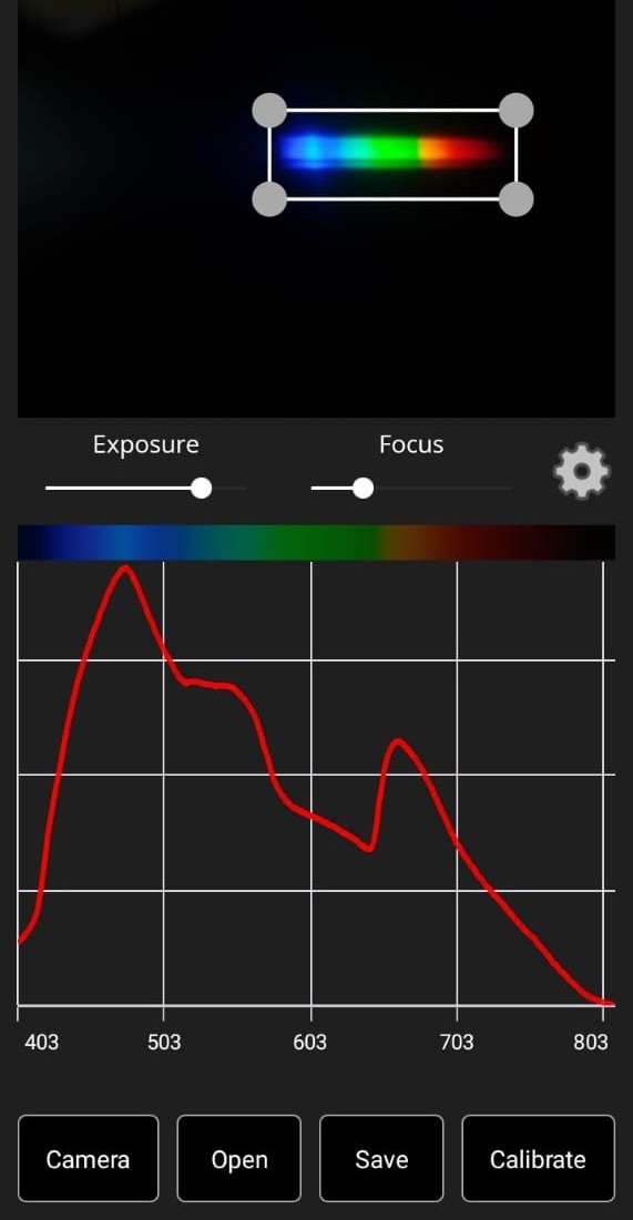
Figure 3: Spectrum analysed using the already available application.
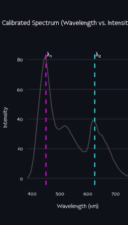
Figure 4: Spectrum analysed using the application developed in this project.
Conclusion
This project successfully illustrates the potential of building a low-cost, portable, and customizable spectrometer by integrating 3D-printed components with smartphone-based sensing. By combining fundamental concepts of optics with practical design and digital tools, we have created a device that not only serves educational purposes but also holds promise for basic analytical applications. The simplicity and accessibility of this setup make it especially valuable for learning environments and resource-constrained settings, where traditional spectrometers may not be readily available. At the same time, its modular design opens the door for a wide range of enhancements. One particularly exciting direction for future development is the incorporation of a photonic crystal. Integrating such a component could significantly improve the spectral selectivity and sensitivity of the device, enabling more precise analysis of reflected or transmitted light. This would elevate the spectrometer’s capabilities, especially in applications involving surface-level sensing or optical filtering. Further improvements could include refining the optical alignment, enhancing spectral resolution, miniaturizing the overall footprint, and introducing machine learning algorithms for real-time spectrum classification and interpretation. In summary, this project demonstrates that meaningful scientific tools can be made both affordable and adaptable, encouraging deeper exploration, innovation, and learning in the field of optics.
Acknowledgement
Sincere gratitude is extended to all those who provided support and guidance throughout the course of this work. Foremost appreciation is due to Dr. Shiva Kiran Bhakta, Teacher-in-Charge, for invaluable guidance, constant encouragement, and insightful suggestions that shaped the direction and quality of the work. Special acknowledgement is given to Mr. Somnath Pandit, Research Scholar, for consistent support, patience, and constructive feedback at every stage of the project. Thanks are also due to the research scholars in the lab for fostering a collaborative and intellectually stimulating environment. Their assistance, technical insights, and camaraderie contributed greatly to the smooth progress of the work. Gratitude is also expressed to the Department of Physics, Indian Institute of Technology (IIT) Kharagpur) for providing the infrastructure, academic resources, and conducive environment necessary for the research. Continued collaboration with IIT Kharagpur is anticipated in future endeavors.
Spectrometer Components
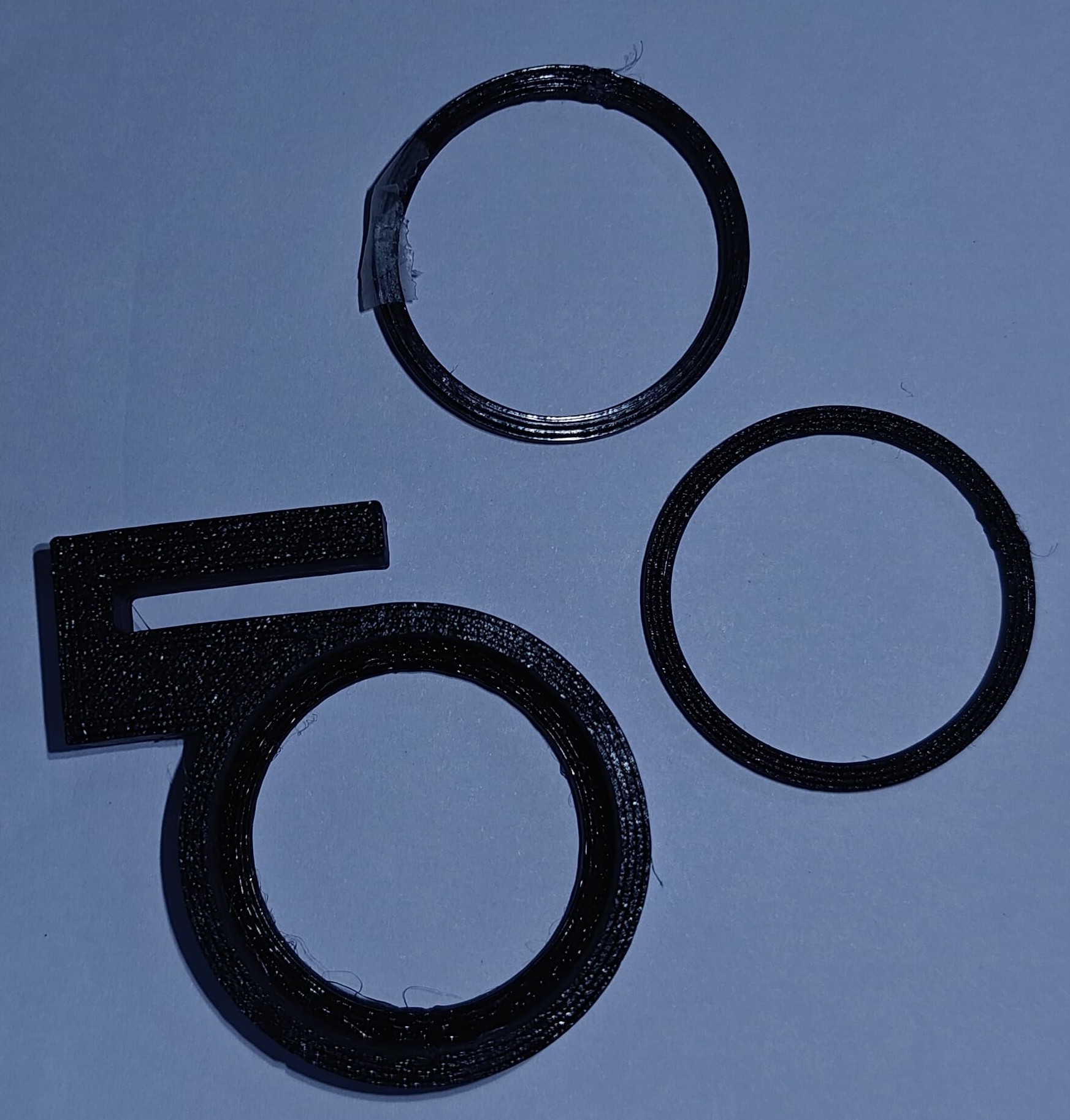
Lens holder
Cuvette holder
Mirror holder
Apertures
Light source area
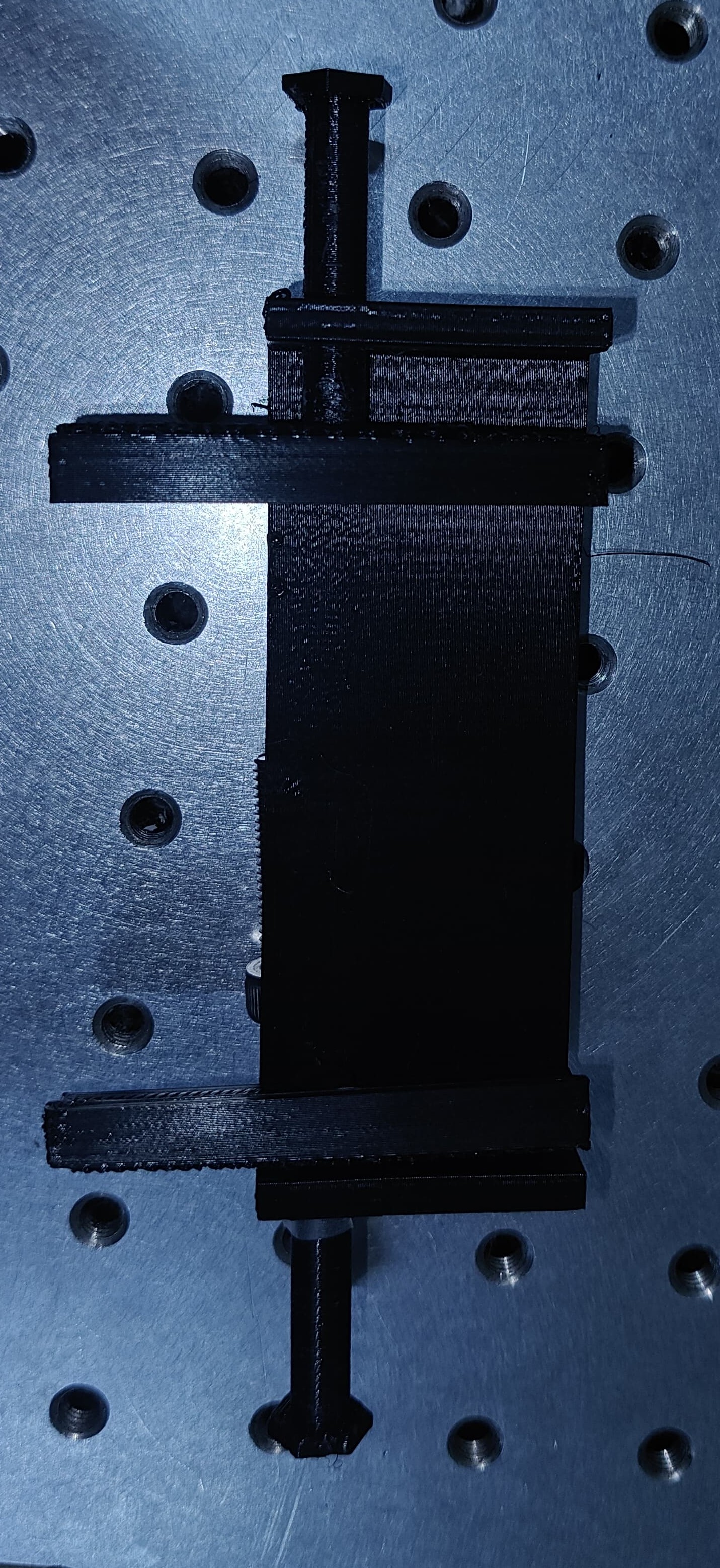
Phone holder
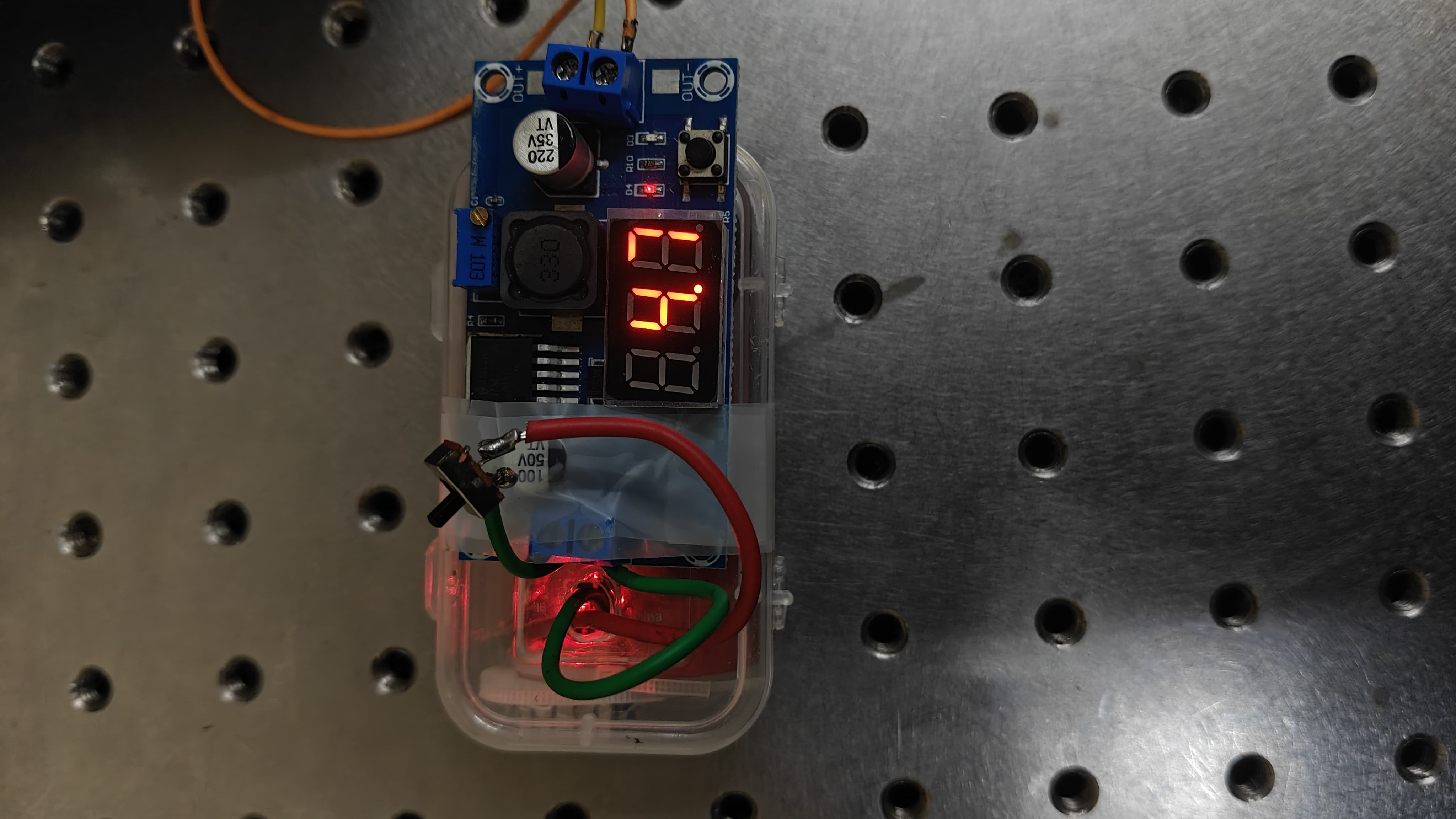
Rechargeable battery
References
- J. D. Joannopoulos et al., Photonic Crystals: Semiconductors of Light. Link
- F. Giorgis et al., "Experimental determination of the sensitivity of Bloch Surface Waves based sensors," Optics Express, vol. 18, no. 8, 2010, DOI
- R. V. Nair and R. Vijaya, "Photonic crystal sensors: An overview," Progress in Quantum Electronics, vol. 34, no. 3, 2010, DOI
- Hackaday, "A Low-Cost Spectrometer Uses Discrete LEDs And Math," Link
- Sai Spectrum, "A web application for the analysis of the spectrum," GitHub